Full articles
The complete text of all ten articles, rendered as static HTML so search engines and AI answer engines can read them without executing JavaScript. Select a card above for the focused single-article view.
Why Your PCB Layout Decides Whether Auto Insertion Ever Pays Off
Board Design
2026-06-24
7 min read
S3010A
In this article
- The machine is not the bottleneck
- What is actually happening
- The tolerance stack nobody budgets for
- Four numbers that decide everything
- Where this becomes a machine decision
- How the gains compound
- Your next step
Most THT automation projects fail on the drawing board, not on the shop floor. Here is what the machine actually needs from your layout — and the four numbers that decide it.
The machine is not the bottleneck
A radial inserter rated at 12,000 CPH will not deliver 12,000 CPH on a board that was designed for hand assembly. It will deliver whatever the layout permits — sometimes less than half the rated figure — and the shortfall shows up as unexplained downtime rather than a clean engineering answer.
This is the single most expensive misunderstanding in through-hole automation. Buyers compare inserter speeds, then discover the constraint was never the head. It was the hole span, the datum holes, the clearance around a capacitor, the warp in the panel.
What is actually happening
Automatic insertion is a tolerance-stacking problem. Five independent error sources have to sum to less than the clearance available:
- Machine positioning tolerance and repeatability
- Workboard holder accuracy — how precisely the board is located
- Board pattern accuracy — where the holes actually are, not where the CAD file says
- Component lead condition — straightness, tip configuration, plating
- Hole diameter and position tolerance
The tolerance stack nobody budgets for
Insertion hole position tolerance is typically ±0.07 mm. Datum hole position tolerance is tighter, around ±0.05 mm. Neither is generous. If your fabricator works to ±0.1 mm on hole position, no amount of machine accuracy will rescue the yield — the error is already spent before the board reaches the machine.
This is why the design guideline conversation has to happen before the purchase order, not after. A layout review costs an afternoon. A line that cannot reach rated speed costs years.
Four numbers that decide everything
Strip away the diagrams and the whole discipline reduces to four quantities:
- Hole diameter. Lead diameter plus 0.48 mm, ±0.08 mm. Too small degrades insertion reliability; too large leaves the component loose and the clinch unreliable.
- Hole span. For radial 2.5 mm components, 2.54 mm. For 5.0 mm components, lead diameter plus 4.5 mm. For 7.5 mm and 10.0 mm components, lead diameter plus 7.04 mm and 9.58 mm respectively.
- Datum hole diameter. Minimum 3.17 mm, recommended 3.96 mm, maximum 6.35 mm — and on Pass-Thru II board handling, 4.74 mm absolute maximum.
- Board thickness. 0.8 mm to 2.36 mm for radial, axial and DIP insertion. Single-board-transfer handling narrows that to 1.52–2.36 mm.
Where this becomes a machine decision
Once the layout is right, the equipment choice becomes straightforward. A 2.5 mm/5.0 mm tooling platform covers the overwhelming majority of radial electrolytics and disc capacitors on consumer and power boards. When pitch needs to move — and it often does — the platform has to be able to accept 7.5 mm and 10.0 mm components without a tooling changeover that eats the shift.
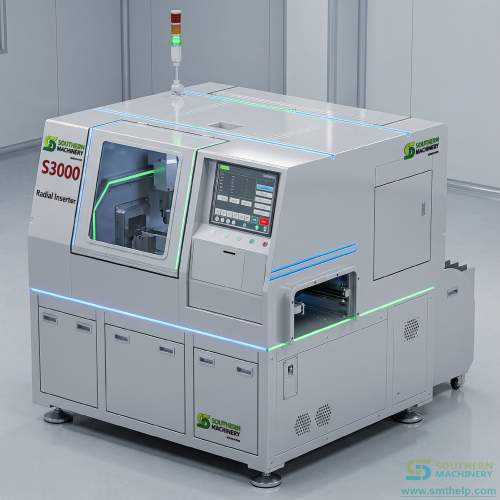
The S3010A radial platform is built around that 2.5 / 5.0 / 7.5 / 10.0 mm tooling envelope with up to ten feeder positions, so a board family with mixed capacitor pitches runs on one setup rather than three.
How the gains compound
A layout that respects these rules keeps paying after commissioning. Changeover drops because datum holes are standardised — the same workboard holder accepts a whole board family. First-pass yield rises because the tolerance stack has margin instead of being exactly spent. And re-layout for the next product generation starts from a template instead of a blank sheet.
The opposite also compounds, in the wrong direction. Every new product re-opens the same argument, and the engineering team quietly learns to design around the machine instead of with it.
Your next step
Before you shortlist any machine, run your current board through a layout review against the four numbers above. If you want a starting point, the design guideline below covers every dimension — axial, radial and DIP — with the formulas and footprint clearances we use in field evaluation.
If you would rather have us do the first pass: send a top-side PCB image, your capacity requirement, and the panel dimensions. You will get a component-by-component insertion verdict — which parts run, which need a pitch change, and which genuinely cannot be automated.
Keywords: THT design guidelines PCB layout auto insertion through hole design rules
The 0.48 mm Rule That Quietly Sets Your Insertion Yield
DFM Rules
2026-06-18
6 min read
S3010A
In this article
- One number, two failure modes
- Where loose components really come from
- The formula, and the exception
- A worked example from a real board
- Where the rule gets enforced
- Why getting this right early matters twice
- Your next step
Hole diameter looks like a trivial detail. It is the difference between a component that clinches tight and one that falls out on the conveyor. Here is the formula and where it breaks.
One number, two failure modes
Ask ten engineers what hole diameter to use for a 0.6 mm lead and you will get ten answers, most of them inherited from a previous employer. But the tolerance is narrow and it fails in both directions.
Undersized holes degrade insertion reliability — the lead catches, the head mis-seats, the machine flags a fault. Oversized holes let the component sit loose in the board, the clinch has nothing to bite against, and parts drop out during wave soldering or handling.
Where loose components really come from
A component that falls out after wave soldering is usually diagnosed as a soldering problem. It is almost always a hole diameter problem. If the hole is larger than recommended, the lead has lateral freedom before clinching. The clinch tooling closes on a lead that is not against the jaw reference surface, and the resulting bend is inconsistent — sometimes holding, sometimes not.
This is why the failure is intermittent and why it resists a simple explanation. The board passes visual inspection, then fails downstream.
The formula, and the exception
For leads captured by the insertion tooling:
Hole diameter = Maximum lead diameter + 0.48 mm ± 0.08 mm
(0.019 in) (0.003 in)
Hole diameter = Maximum lead diameter + 0.58 mm ± 0.08 mm
(0.023 in) (0.003 in)
The exception matters more than the rule. Unguided leads — the ones not captured by the tooling, such as the third leg of a triangular layout, or in-line SIP and potentiometer leads — need a larger clearance because nothing holds them on centre:
For maximum lead diameter, use whichever of the component's dimensional tolerances is largest. Do not average them.
A worked example from a real board
On a 10 W charger panel we evaluated for a Brazilian EMS customer, the specified hole diameters were consistently below the requirement. One electrolytic with a 0.6 mm ± 0.05 mm lead called for a 1.083 mm hole; the board was drilled at 1.6 mm. That is 0.5 mm of unnecessary clearance — enough for the component to sit visibly loose before clinching.
Across the ten components on that panel, the required diameters landed between 0.883 mm and 1.483 mm. None of them needed anything exotic. They needed the formula applied consistently instead of carried over from an older product.
Where the rule gets enforced
A guideline is only useful if something in the process checks it. The practical approach is to build the check into the panel review: for every through-hole component on the BOM, record lead diameter, required hole diameter, and actual drilled diameter, then flag the deltas. On a ten-component board this takes twenty minutes and catches the errors before tooling is cut.
The S3010A radial platform accepts lead diameters from roughly 0.36 mm to 0.86 mm across its 2.5 mm and 5.0 mm tooling, which covers the range on most power and lighting boards. The constraint is rarely the tooling — it is the drill file.
Why getting this right early matters twice
Hole diameter is fixed at fabrication. Correcting it means new tooling, new panels, new qualification — and a delay measured in weeks. Getting it right the first time costs nothing. Getting it wrong costs the difference between a line that runs at rated speed and one that runs at whatever the layout allows, indefinitely.
There is a second-order effect too. Once a fabricator's drill file is standardised on the correct diameters, every subsequent board in that family inherits the correct value. The cost of the fix is paid once; the benefit is paid every order.
Your next step
Take your highest-volume THT board and check three components against the formula — the largest electrolytic, the smallest disc capacitor, and any unguided lead. If any of them is off by more than 0.1 mm, that is your first yield project.
Send us the component list with lead diameters and we will return a hole-diameter table you can hand straight to your fabricator, with the required values and the current deltas side by side.
Keywords: THT hole diameter formula PCB insertion hole size auto insertion design rules
3.5 mm to 5.0 mm: Fixing Capacitor Pitch Before You Buy a Machine
Case Study
2026-06-11
8 min read
S3010A
In this article
- The panel that looked simple
- The real problem was never the machine
- The evaluation method
- What the ten components actually said
- What this looks like in production
- Why this compounds
- Your next step
A real panel evaluation for a Brazilian power-supply builder. Ten components, three outcomes: runs as-is, needs a packaging change, or cannot be automated. Here is the full table.
The panel that looked simple
A 10 W charger panel: 157.4 mm by 124 mm, 1.2 mm thick, 5.0 mm process edge, twelve units in a 4×3 array. Annual forecast 4.2 million units. Required output 940 UPH, which works out at a 38.3 second panel cycle time.
On paper this is the easiest possible automation candidate. High volume, small panel, standard components. The evaluation told a different story — not because the board was hard, but because the drill file and the packaging had drifted from the design intent over several product generations.
The real problem was never the machine
Ten components needed to be inserted. Three of them were fine. Three needed a pitch or packaging change. Three could not be automated without a component change. One was marginal.
The interesting part is that none of the failures were mechanical. They were all upstream: a capacitor bought in a 3.5 mm pitch when the board was laid out for 5.0 mm, an inductor supplied in bulk when the feeder needs radial tape, a resistor with heat-shrink sleeving that has no handling surface for a gripper.
The evaluation method
For every component, four quantities go in and one verdict comes out:
- Current pitch — the lead spacing the component is supplied in
- Current PCB pitch — the hole spacing on the board as drilled
- Required PCB pitch — what the tooling needs
- Lead diameter and required hole diameter — checked against the 0.48 mm rule
The verdict falls into four buckets: runs as-is, adapt the pitch, change the packaging, or does not fit. That last bucket is not a failure of the evaluation — it is the most valuable output, because it tells you where manual labour will remain and lets you plan for it instead of discovering it at commissioning.
What the ten components actually said
Results from the 10 W panel, with the original Portuguese-language engineering notes:
Six of nine run on the radial platform with no change. One needs a pitch adaptation on the panel. One needs a packaging change at the component supplier — a commercial action, not an engineering one. Two stay manual.
| Ref | Component | Current pitch | Required pitch | Verdict |
|---|
| EC101, EC102 | Electrolytic capacitor | 3.5 mm | 5.0 mm | Adapt pitch to 2.5 mm |
| EC201 | Electrolytic capacitor | 2.5 mm ± 0.05 | 2.5 mm | Runs as-is |
| EC202 | Electrolytic capacitor | 2.5 mm | 2.5 mm | Runs as-is |
| EC103 | Electrolytic capacitor | 2.5 mm | 2.5 mm | Runs as-is |
| CY101 | Safety capacitor | 10.0 mm ± 1.00 | 10.0 mm | Runs as-is |
| L101 | Axial inductor | Axial tape | 5.00 mm | Change to radial tape packaging |
| FR101 | Fusible resistor | Bulk | 12.5 mm | Does not fit — heat-shrink sleeving, bulk supply |
| USB1 | USB-A connector | Odd-form | — | Does not fit — odd-form, tray |
| TR1 | Transformer | Odd-form | — | Does not fit — odd-form, tray |
What this looks like in production
The S3010A accepts 2.5 mm, 5.0 mm, 7.5 mm and 10.0 mm tooling on one platform, so the mixed pitches on this panel do not require a tooling changeover between products. That is the difference between a line that runs a mixed family on one setup and a line that stops three times a shift.
The two odd-form parts — the USB-A connector and the transformer — are a different problem. They are gripper-fed, tray-presented components, which is exactly the S7900 odd-form territory rather than the radial platform. Splitting them across two machines is the correct answer for this board, and it is better to know that during evaluation than during ramp.
Why this compounds
The panel evaluation is reusable. The 20 W charger in the same family shares four component references with the 10 W. Once the pitch corrections are made for one, they carry to the other. By the third product generation, the component library is largely pre-validated and the evaluation becomes a checklist rather than a project.
The reverse is also true. A supplier change that silently alters pitch or packaging reintroduces the whole problem. Which is why the pitch and packaging columns belong in the component master data, not in a one-off spreadsheet.
Your next step
Send us a panel drawing plus the component list with part numbers. We will return the same four-column verdict table — runs as-is, adapt pitch, change packaging, or stays manual — with the required hole diameters calculated against the 0.48 mm rule.
If you have a panel already in production, the more useful exercise is the reverse: tell us your current UPH and we will show you which of the three constraint categories is capping it.
Keywords: capacitor pitch auto insertion THT DFM evaluation radial insertion pitch
Your Resistor Leads Are Too Short, And It Is Costing You the Line
Axial Insertion
2026-06-04
7 min read
S-4000 / S-4000H
In this article
- A failure that looks mechanical but is not
- Why the span keeps being wrong
- The formulas
- Two limits that catch people out
- Where the rules are enforced
- The compounding effect
- Your next step
Axial insertion fails for one reason more than any other: the hole span is smaller than the component body needs. The formula is simple and almost nobody applies it.
A failure that looks mechanical but is not
When an axial inserter damages a component body during insertion, the instinct is to blame the driver tip or the machine setup. In most cases the machine is doing exactly what it was told — the board simply does not have enough space between the two holes for the body that has to sit there.
The driver tips come down either side of the body. If the hole span is too small, the body has nowhere to go and the tips close on it. The damage is immediate and visible, which is at least honest — unlike the yield losses that come from a span that is marginal rather than clearly wrong.
Why the span keeps being wrong
Designers calculate hole span from the component's nominal body length plus a small margin. That is the right instinct applied to the wrong quantity, because the tolerance that matters is the maximum body length, not the nominal — and for non-symmetrically shaped components there is an additional correction.
There is a second reason. Component vendors change body dimensions between production lots without changing the part number. A span that worked for three years can fail without any design change on your side.
The formulas
Minimum insertion hole span is a function of body length, tooling style and lead diameter. Four tooling families, four formulas:
Standard tooling Min span = [(Body length x 1.112) + 2.36 mm] - Lead dia
Large lead tooling Min span = [(Body length x 1.085) + 4.11 mm] - Lead dia
5 mm tooling Min span = [(Body length x 1.109) + 1.40 mm] - Lead dia
5.5 mm tooling Min span = [(Body length x 1.067) + 2.30 mm] - Lead dia
Non-symmetrical components: subtract a further 0.41 mm from max body length
Two operating rules follow from this. First, design the span greater than the calculated minimum, never equal to it — body lengths vary between lots. Second, keep the span consistent across consecutive insertions, because lead scrap problems appear when span changes too fast.
Two limits that catch people out
Body diameter. In axial insertion the overall form length is fixed, so board thickness and body diameter compete for the same space:
Max body diameter = Fixed form length - (2 x board thickness)
Standard / high density / large lead tooling: form length 10.69 mm
5 mm / 5.5 mm tooling: form length 11.68 mm
Example: 1.57 mm board, standard tooling
Max body dia = 10.69 - (2 x 1.57) = 7.55 mm
At a 5 mm insertion span, the maximum body diameter collapses to 2.29 mm and the maximum lead diameter to 0.61 mm. This is a genuinely tight window, and it is where a lot of 'the machine cannot handle our parts' complaints originate.
Span stability. On the 6295, 6292 and 6287 series, insertion span across five consecutive insertions should not vary by more than 10 mm. On the 6241, the limit is 5 mm across two consecutive insertions. Boards that mix a 7.5 mm resistor and a 22 mm wire link in adjacent positions can trip this.
Where the rules are enforced
The S-4000 axial platform and the S-4000H jumper wire variant share this tooling discipline. Jumper wire insertion in particular is sensitive to span variation because the wire is formed rather than supplied pre-formed — the tooling does the forming, so span accuracy is not just about clearance, it is about the shape of the finished link.
Practically, this means jumper wire patterns should be grouped by span in the layout, with the widest span variation kept within the operating limit rather than distributed across the board.
The compounding effect
Hole span is set in the CAD library. Fix the footprint for a given body length once and every board that uses that footprint inherits the fix — permanently, across every future product. This is the highest-leverage correction available in THT design, because it is made once and applied indefinitely.
The cost of not fixing it is also compounding, in the form of an engineering team that treats axial insertion as unreliable and quietly routes axial components to manual assembly. That decision is made gradually and is rarely revisited.
Your next step
Pull the axial components on your highest-volume board and calculate the minimum span for each using the standard tooling formula. Compare against the actual hole span. Anything within 0.5 mm of the minimum is a latent problem — fix it before the next component lot arrives.
If you have a jumper wire pattern that keeps failing, send the pattern drawing. Span variation is usually visible immediately, and the fix is normally a layout regroup rather than a tooling change.
Keywords: axial insertion hole span resistor lead length axial auto insertion design
Clinch Angles Explained: Why 45° Is Not Automatically Better
Clinch & Cut
2026-05-28
6 min read
S3010A / S7020T
In this article
- The step everyone skips
- What actually goes wrong
- The specification, precisely
- Where this gets decided
- How the discipline compounds
- Your next step
Clinch angle and clinch length are set independently, and the wrong combination either blocks the hole or fails to hold the part. Here is how to specify both.
The step everyone skips
Between insertion and wave soldering there is a mechanical operation that determines whether the component stays put: clinching. The lead is cut to length and bent against the board so the component is held in place for soldering.
It is specified by two independent numbers — angle and length — and in most design reviews neither is written down. The result is that clinch behaviour varies between machines, between products, and sometimes between shifts.
What actually goes wrong
Three failure modes, all traceable to unspecified clinch parameters:
- Lead overlaps a pad or trace. A long clinch on a dense board bends the lead across a neighbouring conductor. This is a short-circuit risk that passes visual inspection at the clinch station and fails at electrical test.
- Component lifts during handling. A short clinch with a shallow angle does not generate enough retention force. The part survives the clinch station, then shifts on the conveyor or in the wave.
- Inconsistent bend between units. Angle varies with lead hardness and hole diameter, so an unspecified angle drifts with component lot. Some units hold, some do not.
The specification, precisely
For axial insertion, clinch angle is adjustable across 0° to 45°. Clinch lead length is adjustable from 1.28 mm to 1.80 mm, measured from the centre of the insertion hole to the end of the lead. Both are tooling parameters — changing either requires a tooling change, not a software setting.
For DIP and socket insertion the picture is more constrained:
Two notes that are easy to miss. First, tooling change is required to change clinch angle or length — this is not a programmable offset. Second, the achieved angle may vary depending on lead hardness and hole diameter, so the specified figure is a target, not a guarantee.
| Parameter | DIP module | DIP socket | Note |
|---|
| Inward clinch angle | 20° +8° | 0° +10° / −0° | Socket angle is tighter to avoid bushing damage |
| Outward clinch | Available | Not recommended | Explicitly not recommended for socket insertion |
| Minimum lead dimension | 1.02 mm (0.040 in) | 1.02 mm (0.040 in) | Measured at the clinch point |
| Clinch length tolerance | 0.64 ± 0.13 mm | 0.64 ± 0.13 mm | 0.025 ± 0.005 in |
Where this gets decided
Cut-and-clinch is integrated into the insertion head on radial platforms, which means the footprint of the clinch anvil has to be respected in the bottom-side layout, not just the top-side component placement. This is the most commonly overlooked clearance in THT design: the board looks fine from the top and the anvil collides with a neighbouring solder joint from below.
On the S3010A radial platform, cut-and-clinch is part of the standard insertion cycle — the lead is trimmed and formed in the same motion as insertion, so there is no separate clinch pass and no opportunity for the component to shift between operations. The S7020T terminal insertion platform applies the same principle to reel-fed terminals, where clinch geometry determines the mechanical joint quality rather than just retention.
How the discipline compounds
Once clinch angle and length are specified per component family and recorded in the process sheet, three things improve at once: bottom-side layout clearance becomes checkable, wave soldering defects trace to a known parameter instead of a mystery, and new products start from a validated clinch specification instead of rediscovering it.
The alternative — leaving clinch as an operator judgement — means the process cannot be audited. When a customer asks why a joint failed, the honest answer is that nobody specified it.
Your next step
Pick one board family and write down the clinch angle and length for each through-hole component. If the numbers are not currently recorded anywhere, that is the finding — start there before changing any tooling.
If you are seeing shorts that trace back to clinched leads crossing conductors, send us the bottom-side layout. Clinch anvil clearance is usually visible on the drawing, and the fix is normally a layout adjustment rather than a new tool.
Keywords: clinch angle cut and clinch specification THT lead clinching
DIP Sockets That Refuse to Be Auto-Inserted, And the Three Fixes
DIP Insertion
2026-05-21
7 min read
DIP Insertion
In this article
- The component you did not design
- Three root causes, in order of frequency
- The hole diameter calculation
- Where the socket specification gets enforced
- The compounding benefit
- Your next step
DIP socket insertion fails on lead tip geometry, bushing taper and clinch direction — three things specified by the socket vendor, not by you. Here is what to demand.
The component you did not design
When a DIP socket will not insert automatically, the investigation usually starts on the machine and ends on the socket datasheet. Socket vendors optimise for hand insertion and for the electrical interface — not for the lead tip geometry an automated head needs.
The result is a socket that passes every incoming inspection and fails every insertion attempt. It is the most frustrating category of THT automation problem because the fix is commercial, not technical.
Three root causes, in order of frequency
Across field evaluations, socket insertion failures cluster into three causes:
- Non-tapered bushing. A tapered bushing guides the lead into the socket aperture. A non-tapered bushing contributes directly to reduced insertion reliability — the lead catches on the aperture edge and the head mis-seats. This is a socket specification issue and the single most common cause.
- Squared lead tips. A squared tip is acceptable but a tapered tip is preferred, because the taper self-centres against the hole. With squared tips, hole positional tolerance has to absorb the entire misalignment.
- Outward clinch specified. Outward clinching is explicitly not recommended for DIP socket module insertion. If the process sheet says outward clinch, the socket will be damaged or the retention will be unreliable — and this one is on your process, not the vendor.
The hole diameter calculation
DIP insertion has its own formula because the lead cross-section, not just the diameter, drives the requirement. The minimum hole diameter depends on the effective lead diagonal:
Minimum hole dia = Max lead dia + Hole location tolerance + 0.25 mm
Max lead dia C = sqrt(A^2 + B^2) where A and B are the lead cross-section
Lead tip geometry: tapered tip preferred, squared tip acceptable
Tip radius: 0.36 mm max
Lead dimension: 1.78 mm max / 0.76 mm min (long axis)
1.17 mm max / 0.38 mm min (short axis)
The key point is that a rectangular lead's effective diameter is its diagonal, not its width. A 0.64 mm by 0.38 mm lead has a diagonal of roughly 0.74 mm — noticeably larger than either dimension. Calculating from the width alone is the classic DIP hole sizing error.
Where the socket specification gets enforced
DIP insertion shares the tolerance discipline of the radial and axial platforms: machine accuracy, workboard holder accuracy, board pattern accuracy, and hole positional tolerance all contribute to whether the lead finds the aperture. The socket adds a fifth variable — bushing geometry — which is the only one you can control by purchasing decision rather than by process.
In practice this means the socket AVL should carry two extra columns: bushing taper (yes/no) and lead tip configuration. Two columns, checked once per part number, prevent a recurring class of insertion failure.
The compounding benefit
Socket insertion is one of the few THT operations where a purchasing decision directly sets an engineering outcome. Getting it right once — tapered bushing, tapered tip, inward clinch — means every board using that socket inherits reliable insertion. Getting it wrong means the problem reappears on every new product that reuses the part number, and the socket is usually reused because it passed incoming inspection.
There is a commercial angle too. Socket vendors will supply tapered bushing variants on request, often at no premium, if the requirement is stated at quotation. Stating it later means either a change fee or a permanent hand-insertion operation.
Your next step
Open your DIP socket part numbers and check two things: bushing taper and lead tip configuration. If either is unspecified on the datasheet, request the tapered variant explicitly — this is a five-minute email with a measurable yield effect.
Then check your process sheet for outward clinch on any socket. If it is there, change it to inward. That single correction resolves a failure mode that no amount of machine tuning will fix.
Keywords: DIP socket auto insertion machined pin DIP DIP insertion hole diameter
The Hidden Cost of a Warped Panel
Panel & Handling
2026-05-14
6 min read
BHS / SBT
In this article
- Transfer errors are usually blamed on the conveyor
- The three envelope violations
- Panelisation is a throughput decision
- Where handling gets specified
- Why it compounds
- Your next step
Warpage, panelisation and process edge width are decided at fabrication and rarely reviewed. They are also the most common cause of transfer errors on inline THT lines.
Transfer errors are usually blamed on the conveyor
When an inline THT line stops with a board transfer error, attention goes to the board handling system. Most of the time the handling system is behaving correctly — the board is simply outside the geometric envelope it was specified for.
Warpage, panelisation and edge width are all set at fabrication and all directly determine whether a board transfers reliably. None of them are typically reviewed at the design stage, because the board works fine on a manual line where a person places it by hand.
The three envelope violations
Boards fail board handling in three ways:
- Warpage beyond the tolerance. For axial and DIP insertion, maximum warp is 3.17 mm in both measured axes. For radial insertion the tighter figure applies to one axis: 1.60 mm across the board, 3.17 mm along it. A board that warps 2 mm will pass axial but fail radial.
- Panel size outside the handling window. With board handling, minimum is 100 mm by 80 mm and maximum is 483 mm by 406 mm on single-head machines, or 457 mm by 330 mm on dual-head. Without handling, the insertable area is 457.2 mm square.
- Edge geometry unsuitable for clamping. Non-symmetrical panels and panels without a clean process edge cannot be reliably located. The preferred configuration uses breakaway inserts to give a symmetrical panel with a consistent edge.
Panelisation is a throughput decision
Positioning small boards into multiple breakaway panels raises throughput, because the handling overhead is amortised across more units per transfer. Standardising panel size across a product family reduces changeover time, because the same workboard holder and the same handling setup apply to every board in the family.
The trade-off is that panelisation adds process edge material and increases material cost. The break-even depends on board size and volume, and it is worth calculating rather than assuming.
| Parameter | Specification | Applies to |
|---|
| Board thickness | 0.8 – 2.36 mm | Radial, axial, DIP insertion |
| Board thickness (BHS) | 0.8 – 2.36 mm | Board Handling System |
| Board thickness (SBT) | 1.52 – 2.36 mm | Single Board Transfer |
| Max warpage, one axis | 1.60 mm | Radial insertion |
| Max warpage, both axes | 3.17 mm | Axial and DIP insertion |
| Insertable area, no handling | 457.2 × 457.2 mm | Single and dual head |
| Min board with handling | 100 × 80 mm | Single and dual head |
| Max board, single head | 483 × 406 mm | With board handling |
| Max board, dual head | 457 × 330 mm | With board handling |
Where handling gets specified
The choice between Board Handling System and Single Board Transfer is a layout decision with a thickness consequence. BHS covers the full 0.8–2.36 mm range and supports left-to-right or right-to-left transfer on single or dual head machines. SBT suits same-side in/out layouts but narrows the thickness range to 1.52–2.36 mm — a real constraint if your product mix includes 1.0 mm boards.
Workboard holder choice follows from the same analysis. Custom holders suit large lots with medium-to-high changeover; adjustable holders suit prototype and contract manufacturing with low-to-medium changeover. The wrong choice shows up as either unnecessary changeover time or unnecessary holder inventory.
Why it compounds
Panel standardisation is one of the few THT design decisions that reduces cost in three places simultaneously: handling time, workboard holder inventory, and changeover duration. It also makes the line's performance predictable, because the handling overhead becomes a known constant rather than a per-product variable.
Warpage is less forgiving. A board that warps beyond tolerance is a fabrication problem that reappears on every order, and the usual workaround — slowing the line or adding an operator to seat boards manually — converts an inline line into a semi-automatic one without anyone deciding to make that change.
Your next step
Measure warpage on ten boards from your current production lot, using the axis that matters for your insertion type. If radial, the tighter 1.60 mm figure applies. If any board exceeds it, that is a fabrication conversation, not a machine conversation.
Then check your panel size against the handling window. If you are outside 483 × 406 mm or below 100 × 80 mm, the panel needs rework before any handling specification will hold.
Keywords: PCB warpage auto insertion panelisation THT board handling design
Datum Holes: The 3.96 mm Detail That Saves Minutes Every Changeover
Board Design
2026-05-07
6 min read
Workboard Holders
In this article
- The most boring decision with the biggest payoff
- Why changeover keeps costing more than it should
- The specification
- Where the reference is applied
- The compounding effect
- Your next step
Datum holes are the reference the whole insertion process is measured from. Standardise them and changeover collapses. Skip it and every new product pays the setup cost again.
The most boring decision with the biggest payoff
Nothing in THT design is less interesting than datum hole diameter and placement. Nothing else delivers as much changeover reduction for as little effort.
Datum holes are the locating references the board is positioned against. Every other hole on the board is drilled relative to them, and the workboard holder clamps the board by them. If two boards in a family share datum hole diameter and spacing, they share a workboard holder — and changeover between them costs nothing.
Why changeover keeps costing more than it should
Changeover time is usually attributed to programming and feeder setup. Both are real, but the largest single component is often holder change: removing one workboard holder, fitting another, re-datuming, and verifying position.
This is entirely avoidable. It persists because datum holes are designed per product by whoever is working on that product, with no family-level standard. The first board gets 4 mm holes at some spacing; the next gets 3.5 mm at a slightly different spacing; and the holder inventory grows by one every time.
The specification
The tolerances here are tight and they matter:
- Place datum holes with the longest lateral span between them. Angular error scales with span — the wider the baseline, the smaller the positional error at the far end of the board.
- Standardise diameter and spacing across the product family. This is the changeover lever, and it is free.
- If you use Pass-Thru II board handling, the locating hole maximum is 4.74 mm. A 6.35 mm datum hole is fine for standalone operation and out of specification for Pass-Thru II.
- Hold position tolerance at ±0.05 mm. Insertion holes get ±0.07 mm; datum holes are tighter because every other dimension references them.
Four rules follow:
| Feature | Minimum | Recommended | Maximum | Position tolerance |
|---|
| Primary datum hole (D1) | 3.17 mm | 3.96 mm | 6.35 mm | ±0.05 mm |
| Secondary datum hole (D2) | 3.17 mm | — | 6.35 mm | ±0.05 mm |
| Insertion holes (E1–E4) | — | — | — | ±0.07 mm |
| Pass-Thru II handling | — | — | 4.74 mm absolute max | — |
Where the reference is applied
The workboard holder is the physical interface between the datum specification and the machine. A custom holder designed for a specific board size gives the highest positional accuracy and suits large lots with medium-to-high changeover. An adjustable holder accommodates multiple board sizes and suits prototype or contract manufacturing with low-to-medium changeover.
The point is that the holder is a consequence of the datum decision, not a substitute for it. An adjustable holder cannot compensate for datum holes that move between products — it can only accommodate boards that are individually correct.
The compounding effect
A standardised datum scheme turns the workboard holder from a per-product tool into a family asset. The second product on the line skips holder design entirely. The fifth product skips holder design and holder verification. By the tenth product, changeover is programming and feeders only, and the setup time curve flattens.
There is a second benefit that shows up later: when you add a second machine, standardised datums mean boards move between machines without a holder library. That is the difference between a line and a collection of machines.
Your next step
List the datum hole diameter and spacing for every board you currently run. If there is more than one value, you have found your changeover project — standardising on 3.96 mm is the recommended starting point.
If you use Pass-Thru II handling, check that no datum hole exceeds 4.74 mm. That single check prevents a class of transfer errors that is otherwise very hard to diagnose.
Keywords: datum holes PCB workboard holder design THT changeover time
Five Signs Your Odd-Form Components Cannot Be Automated Yet
Odd-Form
2026-04-29
8 min read
S7900 / S7020T
In this article
- Where THT automation projects actually stall
- The five conditions
- What the evaluation looks like
- Where odd-form platforms fit
- Why early evaluation pays twice
- Your next step
Odd-form insertion is where THT automation projects stall. These five conditions decide it — and three of them are fixable without touching the component.
Where THT automation projects actually stall
Radial and axial insertion are solved problems. The components are supplied on tape, the pitches are standard, and the design rules are well established. Odd-form components — connectors, transformers, USB sockets, fuse holders, relays — are where projects stall, because the component was never designed with automated handling in mind.
This produces an uncomfortable conversation. The board needs twelve manual insertion operations, and the customer has budgeted for none of them.
The five conditions
Odd-form automation fails on five conditions. Each is checkable before any equipment is quoted:
- Packaging is bulk or tray with no orientation reference. Bulk components arrive with no consistent orientation. Tray components have orientation, but only if the tray is designed for it — many are not. A feeder needs either a tape format or a tray with a positive orientation feature.
- The component has no handling surface. A gripper needs somewhere to grip that is flat, accessible and does not damage the part. Heat-shrink sleeving, soft moulded bodies and irregular geometry leave nothing to grip. This is the hardest condition to fix, because it usually means a component change.
- Orientation must be identical at insertion. If the component must face a specific way and the packaging does not guarantee that, a vision system has to resolve it — which adds cycle time and cost. Where the packaging can guarantee orientation, vision is unnecessary.
- Polarity is not visually resolvable. If a camera cannot determine polarity from the top surface, the insertion station needs either a mechanical key or a human. Mechanical keys are cheap at the component design stage and expensive afterwards.
- Insertion force exceeds the platform. Heavy transformers and large connectors need insertion force beyond what a standard head provides. This is a real limit and it is better established during evaluation than during commissioning.
What the evaluation looks like
A real panel evaluation makes the pattern clear. On a 20 W charger panel, eleven components were assessed. Nine ran on the radial platform. Two did not:
The useful output is not 'nine out of eleven can be automated'. It is the column that says which two will remain manual, so headcount planning is based on a number rather than an assumption.
| Component | Issue | Fixable? | Action |
|---|
| USB-A connector, tray supplied | Odd-form, no tape format | Partly | Odd-form platform with tray feeder; orientation must be guaranteed |
| Transformer assembly, tray supplied | Odd-form, high insertion force | Partly | Dedicated odd-form station; verify force requirement |
| Inductor supplied in bulk | Bulk packaging | Yes | Change to radial tape — commercial action only |
| Transistor, stick supply | 2.3 mm pitch, stick | No | Stays manual, or re-source in taped format |
| Fusible resistor, heat-shrink | No handling surface | No | Stays manual unless component is re-specified |
Where odd-form platforms fit
Odd-form insertion is a different machine class from radial. Where the radial platform handles taped, standard-pitch components at high cycle rates, an odd-form platform handles the low-volume, high-variety parts — typically with gripper tooling, tray or bowl feeding, and often with vision for orientation.
The S7900 covers that territory with tray, bowl and tube feeding. The S7020T applies the same approach to reel-fed terminals, where the component is a formed metal part rather than an electronic component and the insertion cycle has to produce a mechanically sound joint, not just retention.
For boards with both categories — which is most real boards — the practical configuration is a radial platform plus an odd-form platform, with the manual remainder planned explicitly rather than left as a surprise.
Why early evaluation pays twice
The odd-form decision is largely a purchasing decision. A component supplied in bulk can often be sourced in tape at the same unit price. A component with no handling surface usually cannot be fixed at all. Knowing which is which before equipment selection changes the scope of the project — sometimes substantially.
It also changes the ROI calculation honestly. A line that automates nine of eleven operations is a good investment. A line that was expected to automate all eleven and achieves nine is a project that runs over budget and under-delivers, not because the equipment failed but because the evaluation was skipped.
Your next step
List every through-hole component on your board and mark the packaging format: tape, tray, tube, bulk, stick. Tape and tube are usually straightforward. Bulk and stick are usually the problem. Tray depends entirely on whether the tray has an orientation feature.
Send us the list with part numbers and packaging. You will get back a verdict per component — automatable, automatable after a packaging change, or stays manual — and a realistic count of manual operations for your ROI model.
Keywords: odd form insertion odd form feeder connector auto insertion
From 940 UPH to a Lights-Out THT Line: A Charger Design Audit
Case Study
2026-04-22
9 min read
S3010A / S7020T / S7900
In this article
- The brief
- What the numbers did not show
- Panel geometry and the cycle-time budget
- The component verdicts
- What the line actually needs
- Why the audit is worth more than the quotation
- Your next step
Two charger panels, 5.4 million units a year, 1210 UPH combined. A full design audit showing exactly where automation ends and manual work begins.
The brief
A power-supply builder with two charger panels in the same family. The 10 W panel runs 4.2 million units a year at a required 940 UPH. The 20 W panel runs 1.2 million at 270 UPH. Combined requirement: 1210 UPH across 5.4 million units.
The question was not whether to automate. At that volume the arithmetic is settled. The question was what the line would actually look like, and how much manual work would remain.
What the numbers did not show
Both panels looked like clean automation candidates on paper. Small, high volume, standard components, shared references between the two products.
The evaluation surfaced three categories of constraint that no capacity calculation would have caught:
- Pitch mismatch. Two electrolytics on the 10 W panel were supplied at 3.5 mm pitch against a board laid out for 5.0 mm. The components existed in the right pitch — they simply were not the ones being purchased.
- Packaging mismatch. An inductor supplied in bulk and a transistor supplied in stick format, both of which needed taped supply to run on the radial platform.
- Genuine odd-form. A USB-A connector and a transformer, both tray-supplied, both requiring an odd-form platform rather than a radial one.
Panel geometry and the cycle-time budget
The two panels are similar but not identical, and the difference matters for handling:
Both panels sit comfortably inside the handling window — well above the 100 × 80 mm minimum, well below the 483 × 406 mm maximum. Thickness at 1.2 mm is inside the 0.8–2.36 mm range for both BHS and SBT handling, so handling choice is not constrained here.
The 10 W panel is the throughput driver: 940 of the 1210 combined UPH, on a 38.3 second cycle. That is the panel the line has to be designed around.
| Parameter | Charger 10 W | Charger 20 W |
|---|
| Panel length | 157.4 mm | 185.5 mm |
| Panel width | 124 mm | 157.65 mm |
| Panel thickness | 1.2 mm | 1.2 mm |
| Process edge width | 5.0 mm | 5.0 mm and 10.0 mm |
| Units per panel | 12 (4×3) | 16 (4×4) |
| Annual forecast | 4,200,000 | 1,200,000 |
| Required UPH | 940 | 270 |
| Panel cycle time | 38.3 s | 177.8 s |
The component verdicts
Across the two panels, components fell into three groups. The 10 W results:
The 20 W panel followed the same pattern with one addition: a transistor supplied in stick format at 2.3 mm pitch, which has no taped equivalent at that pitch and stays manual.
| Ref | Component | Current | Required | Verdict |
|---|
| EC101/102 | Electrolytic cap | 3.5 mm pitch | 5.0 mm | Adapt pitch |
| EC201 | Electrolytic cap | 2.5 mm | 2.5 mm | Runs as-is |
| EC202 | Electrolytic cap | 2.5 mm | 2.5 mm | Runs as-is |
| EC103 | Electrolytic cap | 2.5 mm | 2.5 mm | Runs as-is |
| CY101 | Safety cap | 10.0 mm | 10.0 mm | Runs as-is |
| L101 | Axial inductor | Axial tape | 5.0 mm radial | Change packaging |
| FR101 | Fusible resistor | Bulk + sleeving | 12.5 mm | Stays manual |
| USB1 | USB-A connector | Odd-form, tray | — | Odd-form platform |
| TR1 | Transformer | Odd-form, tray | High force | Odd-form platform |
What the line actually needs
Three stations, not one:
- Radial platform for the taped, standard-pitch components — the majority of the component count and the source of the 940 UPH figure. A 2.5 / 5.0 / 7.5 / 10.0 mm tooling envelope covers every pitch on both panels without a tooling changeover, which is what makes the shared family viable.
- Odd-form platform for the USB-A connector and the transformer, using tray feeding. Lower cycle rate, higher component variety, and the right place for gripper tooling.
- Manual station for the fusible resistor with heat-shrink sleeving and the stick-supplied transistor — a small, defined, plannable operation rather than a residual that surfaces at ramp.
Why the audit is worth more than the quotation
The component verdict table is the deliverable that matters. It converts an open-ended automation ambition into a specific scope: this many components on this platform, this many on that platform, this many remain manual, this is the headcount.
It also protects the ROI model. A line designed for the real component set hits its numbers. A line designed for an optimistic component set does not, and the shortfall is usually attributed to the equipment.
And it carries forward. The 10 W and 20 W panels share four component references. Once the pitch and packaging corrections are made for one, they apply to the other — and to the next product in the family.
Your next step
The most useful thing you can send us is what this customer sent: a panel drawing, the component list with part numbers, packaging formats, and your capacity requirement. From that we produce the same three-station recommendation and the same verdict table.
If you want to run the numbers yourself first, the THT insertion ROI calculator and the auto insertion readiness checklist below use the same inputs. Start with the checklist — it will tell you whether a full evaluation is worth commissioning.
Keywords: THT line design audit charger PCB assembly auto insertion ROI